- 您现在的位置:买卖IC网 > Sheet目录1252 > VTERB-DECO-XP-N1 (Lattice Semiconductor Corporation)IP CORE VITERBI DECODER XPGA
�� �
�
�Lattice� Semiconductor�
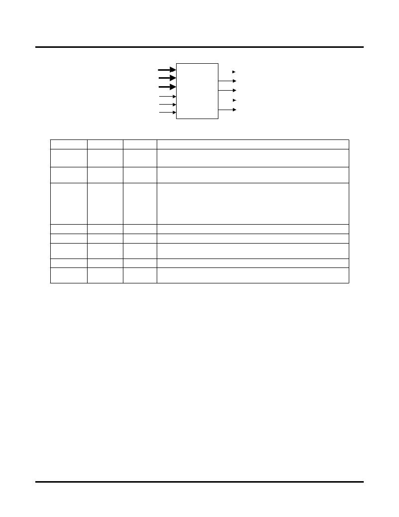
�Figure� 6.� Top� Level� Block� Diagram�
�din_0�
�dout�
�Viterbi� Decoder� User’s� Guide�
�Table� 1.� Core� Signals�
�din_1�
�din_2�
�clk�
�reset_n�
�pd_start�
�Viterbi�
�Decoder�
�valid�
�pd_out�
�ber�
�ber_valid�
�Port�
�clk�
�reset_n�
�pd_start�
�Bits�
�1�
�1�
�1�
�I/O�
�Input�
�Input�
�Input�
�Description�
�System� clock.� The� clock� speed� is� equal� to� the� input� symbol� rate.�
�System-wide� asynchronous� active-low� reset� signal.�
�Punctured� data� block� start.� This� indicates� the� start� of� a� new� block� of�
�punctured� data.� Not� available� while� decoding� non-punctured� codes�
�din_0,�
�din_1,�
�din_2�
�1� or�
�3� to� 8� (each)�
�Input�
�Data� input� buses.�
�?� The� buses� become� one-bit� inputs� for� hard� decision� decoding.�
�?� The� buses� are� equal� to� the� soft� width� for� soft� decision� decoding.�
�?� For� punctured� codes,� the� number� of� buses� is� one.�
�?� For� non-punctured� codes,� the� number� of� buses� corresponds� to� the�
�code� rate:� two� for� 1/2� rate� codes,� three� for� 1/3� rate� codes.�
�dout�
�valid�
�pd_out�
�1�
�1�
�1�
�Output�
�Output�
�Output�
�Decoded� data� output.�
�This� indicates� the� data� currently� presented� on� dout� is� valid.�
�Punctured� decoder� output.� This� indicates� the� data� currently� presented� on�
�dout� is� valid.� Not� available� while� decoding� non-punctured� codes.�
�ber�
�ber_valid�
�16�
�1�
�Output�
�Output�
�Bit-error� rate� output�
�This� indicates� valid� data� is� being� presented� at� the� ber� output� port.� This�
�signal� goes� high� at� the� end� of� every� block� of� BER� Period� clocks.�
�Viterbi� Decoder� Con?guration� Options�
�Con?gurable� Parameters�
�The� following� core� parameters� give� the� user� the� capability� to� tailor� the� core� to� realize� different� con?gurations� of� the�
�Viterbi� decoder.�
�Constraint� Length:� The� value� can� be� any� integer� from� 3� to� 8.�
�Code� Rate:� This� is� the� symbol� output� rate� of� the� encoder,� de?ned� as� the� number� of� output� bits� per� input� bit� in� the�
�encoder.� For� non-punctured� codes,� this� can� be� equal� to� 1/2� or� 1/3.� For� punctured� codes,� this� parameter� de?nes� the�
�code� rate� for� the� mother� code� and� is� ?xed� to� 1/2.�
�Traceback� Length:� This� is� the� length� of� the� survivor� sequence� in� the� traceback� through� the� Viterbi� trellis.� It� can� be�
�any� value� from� 8� to� 128.�
�Generator� Polynomials:� GP0,� GP1� and� GP2� are� generator� polynomials.� GP2� is� only� used� in� non-punctured�
�decoders� with� a� code� rate� of� 3.�
�Implementation� Methods:� In� the� parallel� implementation,� the� processing� of� data� symbols� is� completed� in� one�
�cycle.� In� the� hybrid� implementation,� it� is� completed� in� 2� hybrid� index� cycles.�
�Decoder� Inputs:� The� decoder� supports� hard� and� soft� decision� decoding.� For� soft� decision� decoding,� the� width�
�(soft� width)� can� be� any� integer� from� 3� to� 8.� The� soft� decision� decoder� also� supports� either� signed� or� unsigned� data�
�types.� For� non-punctured� codes,� the� decoder� can� be� con?gured� either� as� a� hard-decision� or� soft-decision� decoder,�
�whereas� for� punctured� codes,� the� decoder� can� only� be� a� soft-decision� decoder.�
�5�
�发布紧急采购,3分钟左右您将得到回复。
相关PDF资料
VTP110F
POLYSWITCH PTC RESET 1.1A STRAP
VTP175LF
POLYSWITCH PTC RESET 1.75A STRAP
VTP210GF
POLYSWITCH PTC RESET 2.1A STRAP
VTP210SF
POLYSWITCH PTC RESET 2.1A STRAP
W51-A121B1-10
CIRCUIT BREAKER THERM 10A ILLUM
W54-XC2A4B10-40
CIRCUIT BREAKER THERMAL 40AMP
WV-089047-10-9
LABEL ID PRODUCTS
XC6T-644
CONNECTR 64POS STRAIN RELIEF DIN
相关代理商/技术参数
VTESALLANF-155.520000
功能描述:155.52MHz LVPECL VCXO Oscillator Surface Mount 3.3V 100mA Enable/Disable 制造商:taitien 系列:VT 包装:剪带 零件状态:新产品 类型:VCXO 频率:155.52MHz 功能:启用/禁用 输出:LVPECL 电压 - 电源:3.3V 频率稳定度:±50ppm 工作温度:-40°C ~ 85°C 电流 - 电源(最大值):100mA 等级:- 安装类型:表面贴装 大小/尺寸:0.276" 长 x 0.197" 宽(7.00mm x 5.00mm) 高度:0.075"(1.90mm) 封装/外壳:6-SMD,无引线(DFN,LCC) 电流 - 电源(禁用)(最大值):- 标准包装:200
VTESFP4G
制造商:Promise Technologies 功能描述:SP.VTRAK.4GB SFP OPTICAL TRANSCEIVER.BOX - Bulk
VTEUALJANF-122.880000
功能描述:122.88MHz CMOS VCXO Oscillator Surface Mount 3.3V 40mA Enable/Disable 制造商:taitien 系列:VT 包装:剪带 零件状态:新产品 类型:VCXO 频率:122.88MHz 功能:启用/禁用 输出:CMOS 电压 - 电源:3.3V 频率稳定度:±50ppm 工作温度:-40°C ~ 85°C 电流 - 电源(最大值):40mA 等级:- 安装类型:表面贴装 大小/尺寸:0.276" 长 x 0.197" 宽(7.00mm x 5.00mm) 高度:0.075"(1.90mm) 封装/外壳:6-SMD,无引线(DFN,LCC) 电流 - 电源(禁用)(最大值):- 标准包装:200
VTEUALJANF-153.600000
功能描述:153.6MHz CMOS VCXO Oscillator Surface Mount 3.3V 40mA Enable/Disable 制造商:taitien 系列:VT 包装:剪带 零件状态:新产品 类型:VCXO 频率:153.6MHz 功能:启用/禁用 输出:CMOS 电压 - 电源:3.3V 频率稳定度:±50ppm 工作温度:-40°C ~ 85°C 电流 - 电源(最大值):40mA 等级:- 安装类型:表面贴装 大小/尺寸:0.276" 长 x 0.197" 宽(7.00mm x 5.00mm) 高度:0.075"(1.90mm) 封装/外壳:6-SMD,无引线(DFN,LCC) 电流 - 电源(禁用)(最大值):- 标准包装:200
VTEUALJANF-30.720000
功能描述:30.72MHz CMOS VCXO Oscillator Surface Mount 3.3V 20mA Enable/Disable 制造商:taitien 系列:VT 包装:剪切带(CT) 零件状态:新产品 类型:VCXO 频率:30.72MHz 功能:启用/禁用 输出:CMOS 电压 - 电源:3.3V 频率稳定度:±50ppm 工作温度:-40°C ~ 85°C 电流 - 电源(最大值):20mA 等级:- 安装类型:表面贴装 大小/尺寸:0.276" 长 x 0.197" 宽(7.00mm x 5.00mm) 高度:0.075"(1.90mm) 封装/外壳:6-SMD,无引线(DFN,LCC) 电流 - 电源(禁用)(最大值):- 标准包装:1
VTEUBLJANF-31.250000
功能描述:31.25MHz CMOS VCXO Oscillator Surface Mount 3.3V 20mA Enable/Disable 制造商:taitien 系列:VT 包装:剪切带(CT) 零件状态:新产品 类型:VCXO 频率:31.25MHz 功能:启用/禁用 输出:CMOS 电压 - 电源:3.3V 频率稳定度:±50ppm 工作温度:-40°C ~ 85°C 电流 - 电源(最大值):20mA 等级:- 安装类型:表面贴装 大小/尺寸:0.276" 长 x 0.197" 宽(7.00mm x 5.00mm) 高度:0.075"(1.90mm) 封装/外壳:6-SMD,无引线(DFN,LCC) 电流 - 电源(禁用)(最大值):- 标准包装:1
VTEUBLJANF-70.656000
功能描述:70.656MHz CMOS VCXO Oscillator Surface Mount 3.3V 30mA Enable/Disable 制造商:taitien 系列:VT 包装:剪带 零件状态:新产品 类型:VCXO 频率:70.656MHz 功能:启用/禁用 输出:CMOS 电压 - 电源:3.3V 频率稳定度:±50ppm 工作温度:-40°C ~ 85°C 电流 - 电源(最大值):30mA 等级:- 安装类型:表面贴装 大小/尺寸:0.276" 长 x 0.197" 宽(7.00mm x 5.00mm) 高度:0.075"(1.90mm) 封装/外壳:6-SMD,无引线(DFN,LCC) 电流 - 电源(禁用)(最大值):- 标准包装:200
VTEUMCJANF-19.440000
功能描述:19.44MHz CMOS VCXO Oscillator Surface Mount 3.3V 10mA Enable/Disable 制造商:taitien 系列:VT 包装:剪切带(CT) 零件状态:新产品 类型:VCXO 频率:19.44MHz 功能:启用/禁用 输出:CMOS 电压 - 电源:3.3V 频率稳定度:±50ppm 工作温度:-20°C ~ 70°C 电流 - 电源(最大值):10mA 等级:- 安装类型:表面贴装 大小/尺寸:0.276" 长 x 0.197" 宽(7.00mm x 5.00mm) 高度:0.075"(1.90mm) 封装/外壳:6-SMD,无引线(DFN,LCC) 电流 - 电源(禁用)(最大值):- 标准包装:1